Scanning probe microscopy
 |
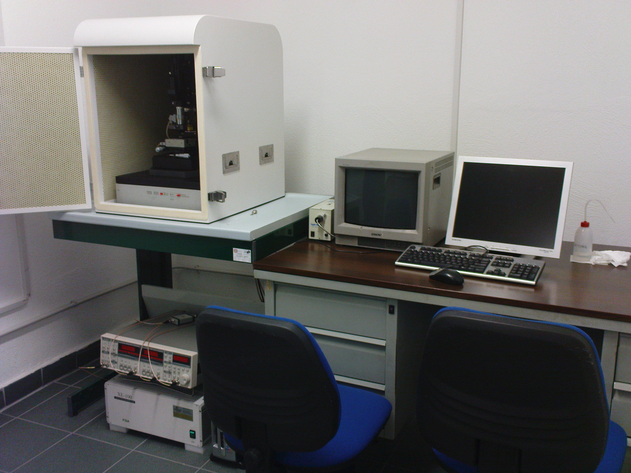 |
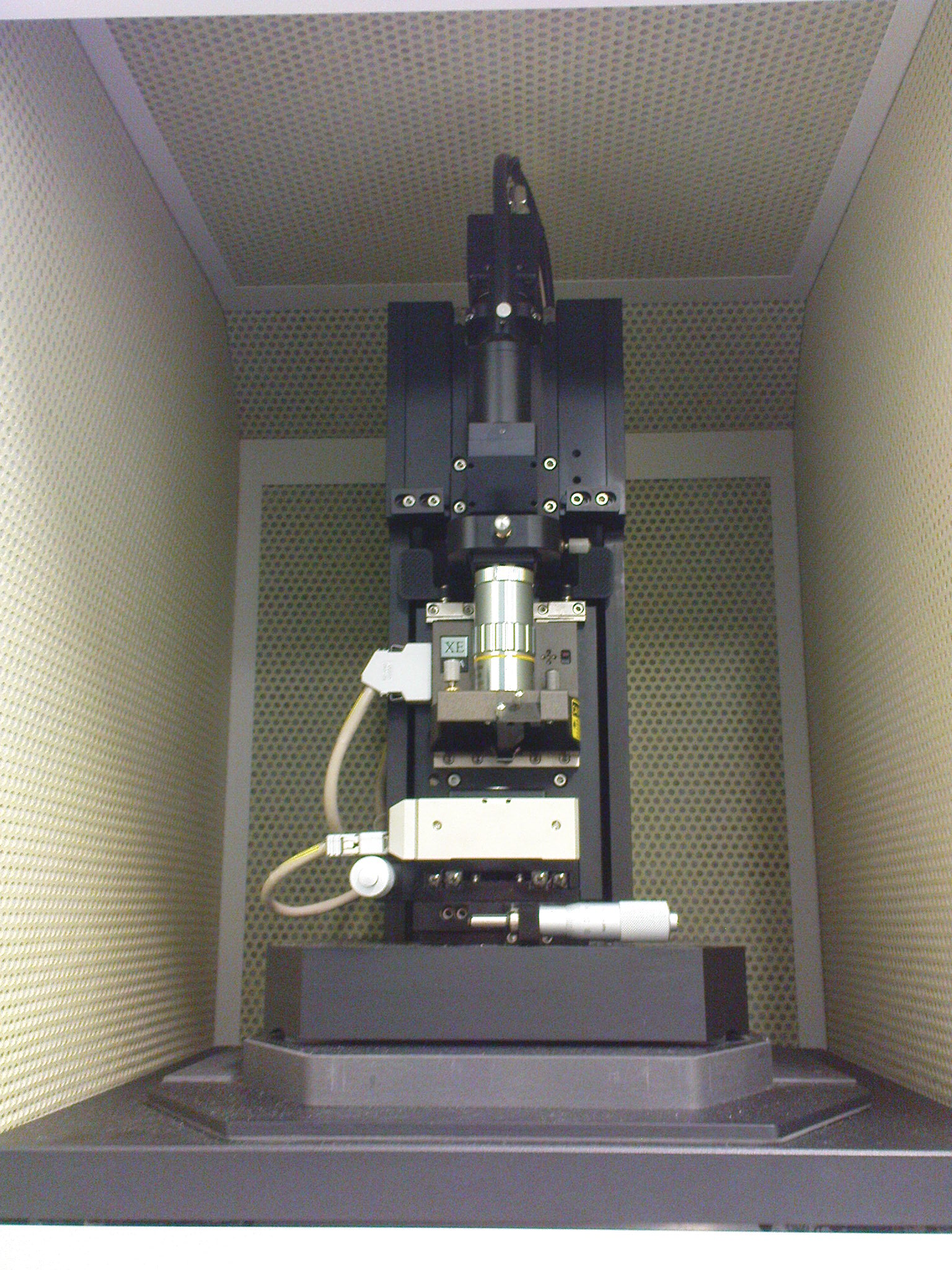
The laboratory of Scanning Probe Microscopy (SPM) is located at the NIS labs of the Innovation Centre in Via Quarello 15/a and is equipped with a XE - 100 system supplied by Park Systems (South Korea). It is, as its main feature, an atomic force microscope (AFM); however, the availability of several accessories allow different scanning probe microscopy techniques to be used.
At present this AFM is fully equipped to perform:
- Contact, intermittent and non contact AFM in both ambient air and liquid environment, Force/Distance spectroscopy
- Lateral force microscopy
- Scanning tunnelling microscopy (STM)
- Electrostatic Force microscopy (EFM), Scanning Kelvin Probe microscopy (SKPM), I/V spectroscopy Conductive AFM (C AFM)
- Nanoindentation
- Nanolithography (Low and high voltage)
Being this AFM microscope part of the NIS instruments, it can be booked by all registered members of NIS.
NEW USERS MUST contact info.nis@unito.it to obtain an access code and Dr. Ettore Bernardi , who is the person in charge of the instrument.
Atomic force microscopy is a member of the scanning probe microscopies family and it has been
discovered in 1986 by G. Binnig, C. F. Quate, and Ch. Gerber (Phys. Rev. Lett. (1986) 56, 930).
It is a powerful tool for imaging, measuring and manipulating matter at the nanoscale,
as it allows accurate information on surface morphology, roughness, mechanical
and electrical properties of different materials to be obtained.
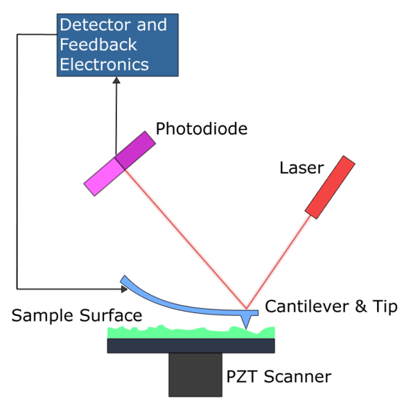 The working principle underlying AFM technique is shown in the figure on the left: a micrometric tip attached to a cantilever
with a low spring constant is brought near the sample surface at a distance ranging from few to a tens of nm. In these conditions,
as a result of this forced interaction, the tip is subjected to a force that can be attractive or repulsive forces depending on
tip-sample distance. The measurement of the interaction force is made possible by tracking the deflection of the cantilever with
the help of a laser beam pointed on the backside of the tip, reflected on a position sensitive photodetector (PSPD) that collects
the upward and downward movements of the tip. The system is able to register the movements of the cantilever, and to transform
them into topographic information in the Z direction; as the sample is mounted on a piezoelectric scanner performing highly
accurate raster on the sample surface in both XY directions, it is possible to obtain a three-dimensional topographic image
of the investigated material.
The working principle underlying AFM technique is shown in the figure on the left: a micrometric tip attached to a cantilever
with a low spring constant is brought near the sample surface at a distance ranging from few to a tens of nm. In these conditions,
as a result of this forced interaction, the tip is subjected to a force that can be attractive or repulsive forces depending on
tip-sample distance. The measurement of the interaction force is made possible by tracking the deflection of the cantilever with
the help of a laser beam pointed on the backside of the tip, reflected on a position sensitive photodetector (PSPD) that collects
the upward and downward movements of the tip. The system is able to register the movements of the cantilever, and to transform
them into topographic information in the Z direction; as the sample is mounted on a piezoelectric scanner performing highly
accurate raster on the sample surface in both XY directions, it is possible to obtain a three-dimensional topographic image
of the investigated material.
The main application of an atomic force microscope is to image the surface of a solid sample at the nanoscale in ambient conditions
(whereas for a scanning electron microscope, vacuum conditions are required).
Unlike the Scanning Tunneling Microscopy, which can analyse only conductive samples, AFM is suitable to image the surface of any solid sample,
regardless of its electronic features.
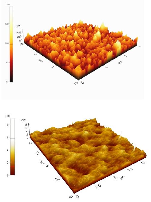 As an example, the picture on the left reports the surface topography of a nanocrystalline CVD diamond film (rms around 6 nm) and of a smooth
homoepitaxially grown film onto a diamond type Ib substrate (rms around 0.3 nm).
These figures have been extracted from a research carried out by our group regarding the role the diamond surface morphology and atomic termination
play in the survival and viability of neuronal cells, which represent an appropriate experimental model for the development of cell-based biosensors.
As an example, the picture on the left reports the surface topography of a nanocrystalline CVD diamond film (rms around 6 nm) and of a smooth
homoepitaxially grown film onto a diamond type Ib substrate (rms around 0.3 nm).
These figures have been extracted from a research carried out by our group regarding the role the diamond surface morphology and atomic termination
play in the survival and viability of neuronal cells, which represent an appropriate experimental model for the development of cell-based biosensors.
It is also possible mapping electrical properties of the sample, using Electric Force Microscopy (EFM) and Scanning Kelvin Probe Microscopy (SKPM ).
In EFM, a conductive cantilever is driven mechanically at a frequency f and electrically at a frequency w, with f much smaller than w; the electric contribution to the cantilever
amplitude at w is extracted using a lock-in amplifier (Single pass EFM).
 In Scanning Kelvin Probe Microscopy (SKPM ), the tip potential is swept by a feed-back loop in order to minimize the electrical force at w.
This value of tip-potential is colllected for every position and it is related to the surface potential of the conductor.
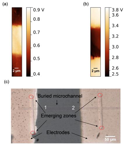
As an example, in the figure on the left is reported the SPKM mapping of a graphitic buried channel in presence of flowing current, the maps referring to surface regions
lying closer to the left (a) and the right (b) electrode.
In Scanning Kelvin Probe Microscopy (SKPM ), the tip potential is swept by a feed-back loop in order to minimize the electrical force at w.
This value of tip-potential is colllected for every position and it is related to the surface potential of the conductor.
As an example, in the figure on the left is reported the SPKM mapping of a graphitic buried channel in presence of flowing current, the maps referring to surface regions
lying closer to the left (a) and the right (b) electrode.
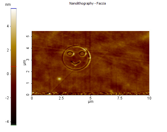 Moreover, it is possible not only to study the surface morphology or the relevant electrical properties, but also to selectively modify surfaces creating nanostructures etc. by means of nanolithography,
performed through application of either excessive force or voltage bias through the tip (Local anodic oxidation, LAO) as shown in the figure on the right.
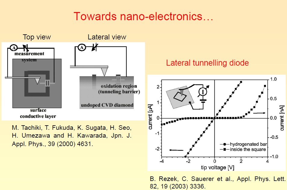
Our group has investigated the Local anodic oxidation (LAO)
process on hydrogenated CVD diamond surfaces in order to draw conductive isolated islands for the fabrication of nano-tunnel diodes
as described in the following figure.
Moreover, it is possible not only to study the surface morphology or the relevant electrical properties, but also to selectively modify surfaces creating nanostructures etc. by means of nanolithography,
performed through application of either excessive force or voltage bias through the tip (Local anodic oxidation, LAO) as shown in the figure on the right.
Our group has investigated the Local anodic oxidation (LAO)
process on hydrogenated CVD diamond surfaces in order to draw conductive isolated islands for the fabrication of nano-tunnel diodes
as described in the following figure.
Useful links: