Scanning Electron Microscopy
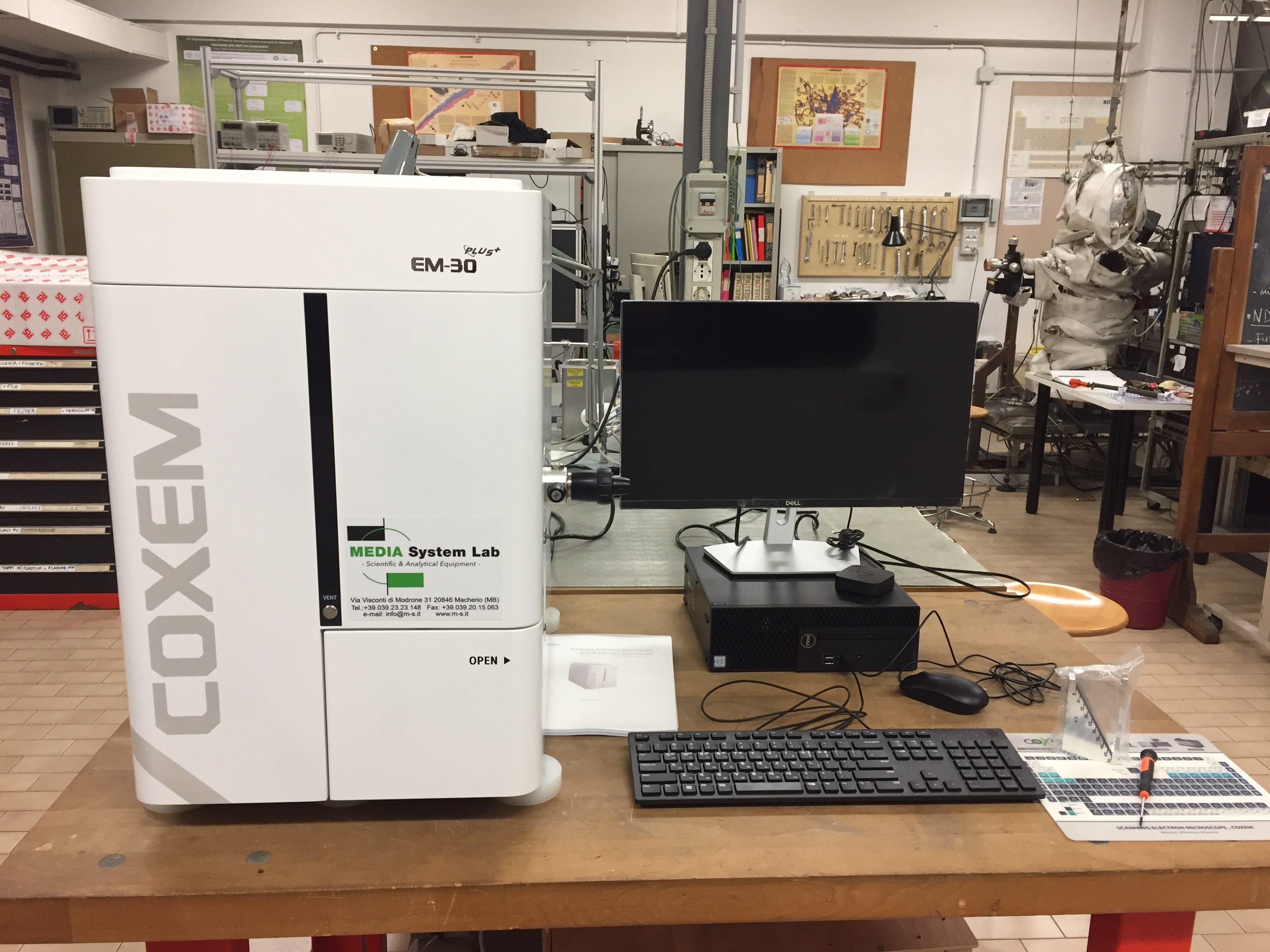
Techniques related to Scanning Electron Microscopy are essential in the field of Material Science, ranging from the morphological characterization of samples and micro-devices (through secondary and backscattering microscopy) to their compositional (through Energy Dispersive Spectroscopy (EDS)) or functional (through Electron Beam Luminescence Spectroscopy (EBIL) ) characterization and for material modification and functionalization (through Electron Beam Lithography (EBL) ). Traditionally, researches at the Physics Department involving the use of scanning electron microscopes are carried out in collaboration with Microscopy Centers in the surroundings: in particular at the "NanoFacility Piemonte" , at the "Centro Conservazione e Restauro La Venaria Reale", at the "Department of Earth Science" or at the "Nanostructured Interfaces and Surfaces (NIS)" Inter-Departmental Center . In July 2019, within the project "Department of Excellence", the Physics Department has acquired a new table-top compact Scanning Electron Microscope COXEM EM-30, equipped with detectors for secondary and backscattering electrons. The microscope is now installed at the Solid State Physics Laboratory, 3rd undergroung floor of the Physics Department and will be used to introduce students to the electron microscopy techniques both in curricular classes and for Bsc, master theses. Moreover, it is available for research activities related to Material Science.