Laser Microfabrication
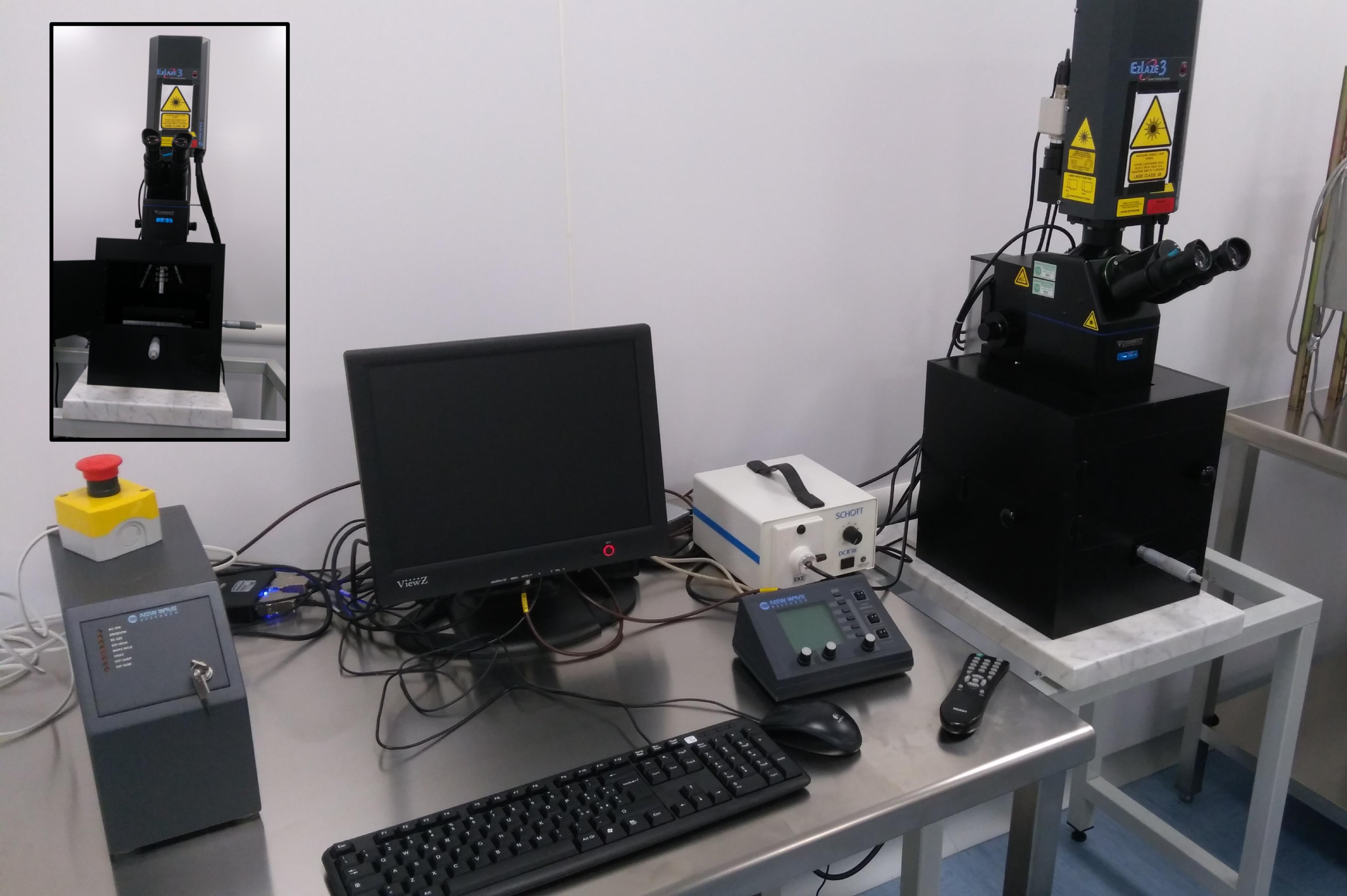
The cleanroom of the Solid State Physics laboratory is equipped with a state-of-the-art apparatus for the microfabrication of materials and devices with a focused high-power pulsed laser.
The strong absorption of high-power focused & pulsed laser from a material can result in an instantaneous thermal shock which can, in turn, induce the local fusion or vaporization of the material. In the latter case, accurate and effective laser ablation can be obtained in short times and micrometric spatial resolution.
Therefore, focused pulsed laser can be employed as an effective tool to perform microfabrication (i.e. micro-ablation) tasks in different classes of materials and devices. The requirement of the sample being absorbing at the employed wavelength is not particularly strict for the process to be effective, since non-linear multi-photon absorption processes can play a significant role at high power densities, even in spectral region where the sample exhibits low optical absorption at the first order.
Alternatively, at low emission intensities and pulse repetitions it is possible to employ the same system to impress UV-sensitive photoresist, thus implementing a photolithography setup operating under room illumination conditions.
The laboratory of the Solid State Physics group is equipped with a ns-pulsed Nd:YAG laser emitting in the IR (1064 nm), VIS (532 nm) or UV (355 nm). The pulse duration is 6 ns and the maximum energy per pulse of 0.6 mJ, resulting in an instantaneous power of 100 kW.
Through a series of dedicated high-power-compatible optics and variable collimating apertures, the laser beam can be focused down to a spot of 1×1 µm2, while the maximum spot size is 25×25 µm2. At the highest demagnification (100× objective), the maximum power density is of the order of ~10 GW cm-2. As mentioned above, at such high power densities, even nominally transparent samples can display strong non-linear absorption and therefore be subjected to ablation.
The quantity (i.e. thickness) of material ablated per single pulse can vary from few nm's to µm's, depending on the irradiation conditions (energy per pulse, number of pulses, focusing conditions, wavelength) and the relevant absorption properties of the material. Lower power densities can result in phase transitions (e.g. local amorphization or induced graphitization in the case of diamond samples) instead of ablation.
The systems adopts a co-axial focusing system for both the laser beam and the sample visualization: therefore it is possible to first identify the point of interest in "microscopy" mode, and then to switch to "laser microfabrication" mode and focus the laser beam on the same spot with micrometric spatial accuracy.
The system is equipped with a fully automatized stage for the sample displacement under the laser irradiation with micrometric spatial accuracy. The PC-controlled system manages both the sample displacement and the laser irradiation parameters (number of pulses, energy per pulse, wavelength) for each spot, therefore it is possible to define arbitrarly complex microfabrication patterns to be reproduced on the sample under processing in a fully automatized protocol.
The system is complemented by a spin coater to implement a UV photolithography setup capable of transferring user-defined patterns on µm-think photoresists.
In the framework of the research on diamond microfabrication, this apparatus is adopted for several different tasks: micro-fabrication of metallic masks for subsequent MeV ion implantations, local ablation of diamond, local graphitization of diamond.